
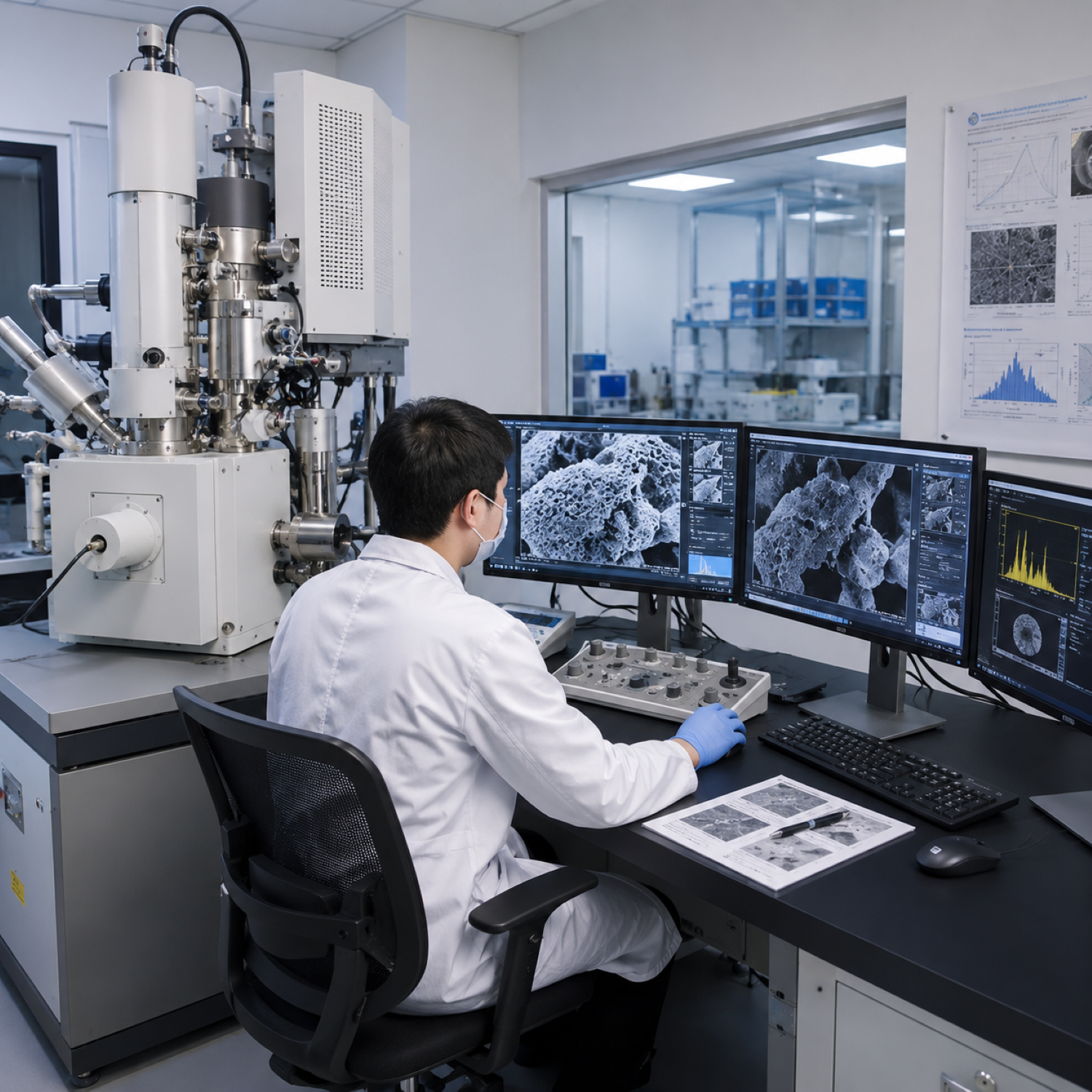
Catch Flaws Early with SEM and Save Your Business Big Time
Understanding the Power of High-Resolution Surface Analysis
When it comes to ensuring product quality and avoiding costly recalls, catching defects early is everything. One of the most reliable tools for this is scanning electron microscopy analysis. This technique allows businesses to detect microscopic flaws invisible to the naked eye or conventional optical microscopes, making it an essential step in quality control and failure analysis.
The ability to analyze surfaces at a nanometer scale helps companies identify structural inconsistencies, contamination, and material defects before these issues escalate into larger problems. Beyond just spotting defects, understanding the root cause at such a detailed level can drastically reduce downtime and warranty claims.
How Scanning Electron Microscopy Improves Quality Assurance Processes
Scanning electron microscopes (SEMs) work by scanning a focused electron beam over the surface of a sample. This interaction generates various signals that can be detected and converted into high-resolution images.
- Surface Morphology – Detailed topographical information revealing cracks, voids, or irregularities
- Material Composition – Using energy-dispersive X-ray spectroscopy (EDS) integrated with SEM allows elemental analysis to detect contamination or incorrect materials
- Dimensional Accuracy – Precise measurements of micro- and nanostructures supporting tight manufacturing tolerances
By incorporating this analysis into manufacturing workflows, businesses can isolate quality issues at an early stage, preventing defective batches from reaching customers.
Step-by-Step Guide to Implementing SEM in Business Operations
Integrating scanning electron microscopy analysis into your quality control system can be tackled in a few clear steps:
- Identify Critical Control Points – Determine which stages in manufacturing or product development require detailed surface inspection
- Sample Preparation – Properly prepare samples for SEM to avoid artifacts; this may include coating with conductive materials for non-conductive samples
- Data Collection and Analysis – Capture high-resolution images and conduct elemental mapping to uncover flaws
- Interpretation and Reporting – Translate microscopy data into actionable insights for engineering and production teams
- Continuous Monitoring – Establish routine SEM inspections aligned with production schedules to maintain control over product quality
Real-World Applications Driving Business Savings
Many industries reap substantial benefits from early flaw detection using SEM. Automotive manufacturers, for example, use this technology to examine engine components for micro-cracks that can lead to premature failure. Electronics companies rely on SEM to check semiconductor wafer surfaces for defects that could impact chip performance.
Delving deeper, there is valuable information found in specialized use cases. For those interested, the details on scanning electron microscopy analysis and its automotive applications provide a concrete example of how this technology translates directly into cost savings and product reliability scanning electron microscopy analysis .
Comparing SEM with Other Inspection Methods
| Method | Resolution | Material Information | Typical Uses |
|---|---|---|---|
| Optical Microscopy | Micrometer scale | No elemental data | Visual inspection of surface defects |
| Scanning Electron Microscopy | Nanometer scale | Elemental and morphological data | Detailed defect analysis, material characterization |
| X-Ray Diffraction | N/A | Crystallographic information | Phase identification and structural analysis |
Challenges and Considerations When Using SEM
While SEM offers unparalleled detail, it requires skilled operators and well-prepared samples to achieve reliable results. The equipment itself demands significant investment and maintenance. However, for businesses with strict quality standards, the upfront costs are outweighed by the reduction in product failures and recalls.
Moreover, integrating SEM findings with production data helps build a comprehensive quality management system, catching issues before they affect end users.
Maximizing ROI Through Early Defect Detection
Applying high-resolution microscopy early in product development or manufacturing stages means fewer defective items and less rework. This proactive approach translates into saved costs and improved customer satisfaction. Using the detailed insights from these analyses, businesses can refine processes, select better materials, or improve design specs to eliminate recurring flaws.
Organizations that invest in this level of scrutiny create a competitive advantage by delivering reliable, high-quality products consistently.